
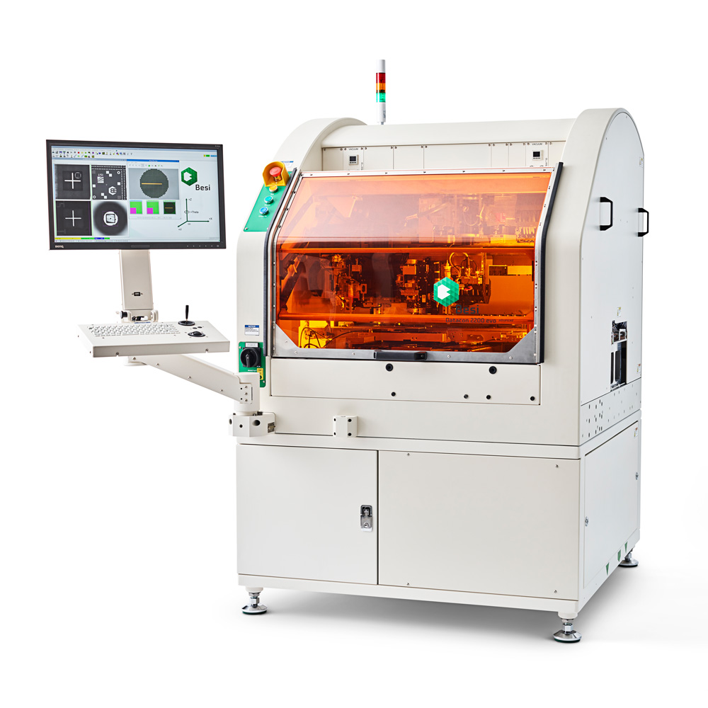
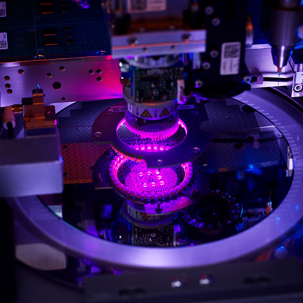
Datacon 2200 evo advanced
The Datacon 2200 evo hS is a high-speed, fully automatic die bonder designed for advanced semiconductor packaging applications.
Featuring precise placement accuracy and versatile bonding capabilities, it supports a wide range of die sizes and materials.
Engineered for maximum throughput and reliability, the Datacon 2200 eco hS is ideal for high-volume production environments requiring consistent quality and efficiency.
More informationThis link leads to an external website.


3 micron Accuracy, @ 3 sigma
± 0.07° Theta placement
2,000 W/cm2 UV curing
99.95% Yield
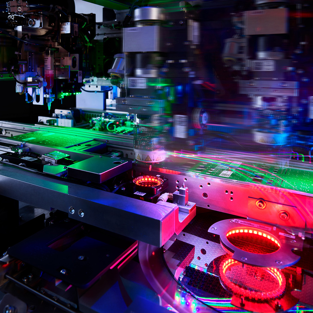
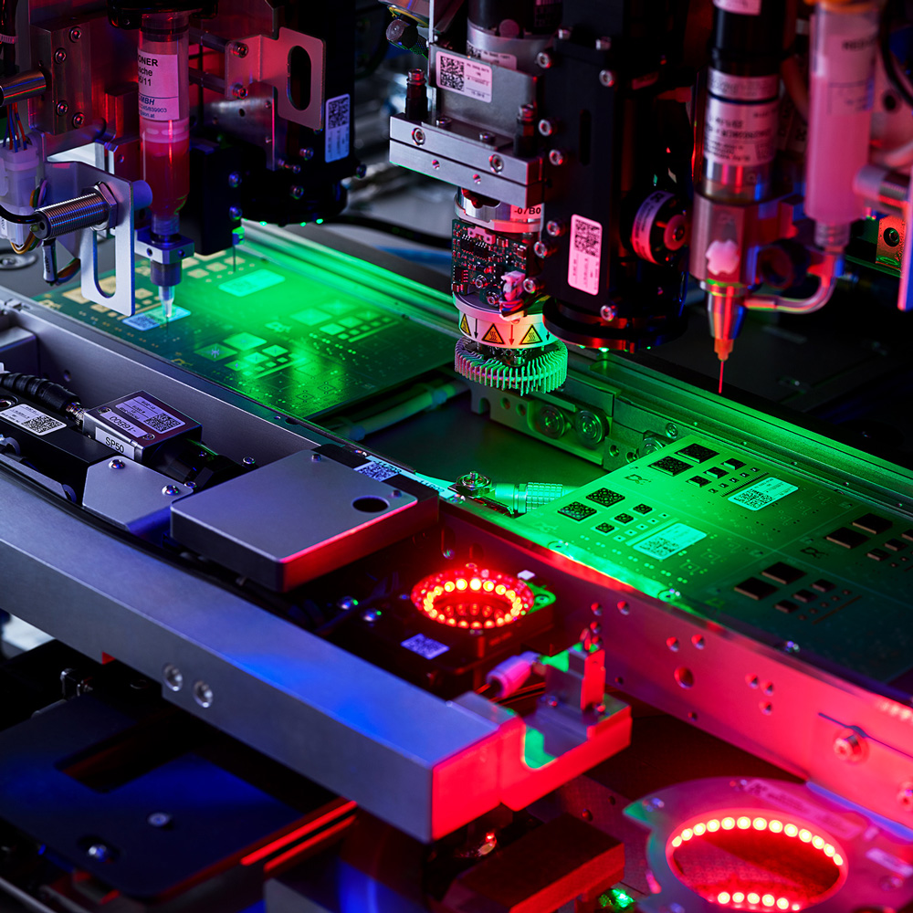
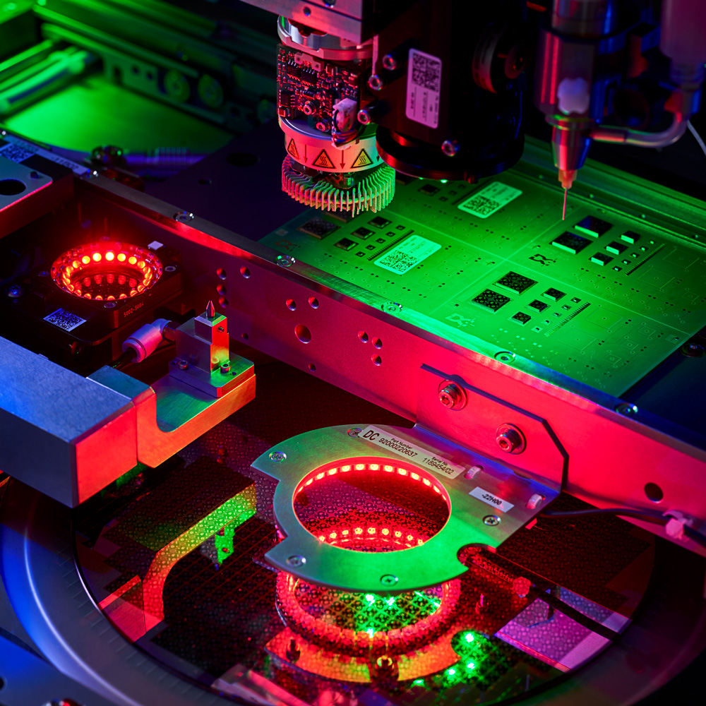
Key Features
Eplore all features of the Datacon 2200 evo advanced
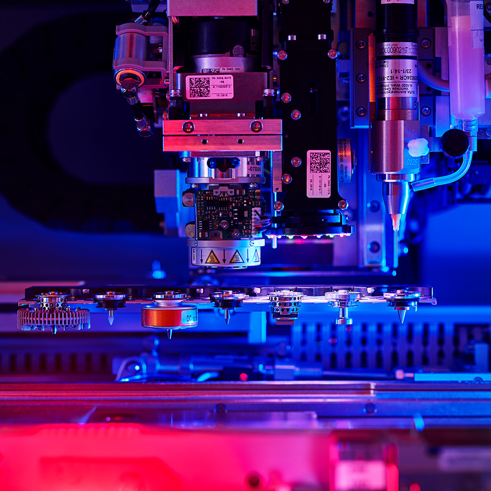
Multi-chip
- Max. 14 different pick up tools / nozzles
- 5 eject tools
- 3 different epoxies / adhesive in a single pass
- Any flip chip / face up die combination
- Dual module for even higher productivity (option)
Accuracy
- ± 3µm @ 3s placement accuracy
- ± 0.07° @ 3s rotational accuracy
- New vision, optics and camera system
- Various configurable (FOV & resolution) set of cameras
- 3D & contactless height measurement options
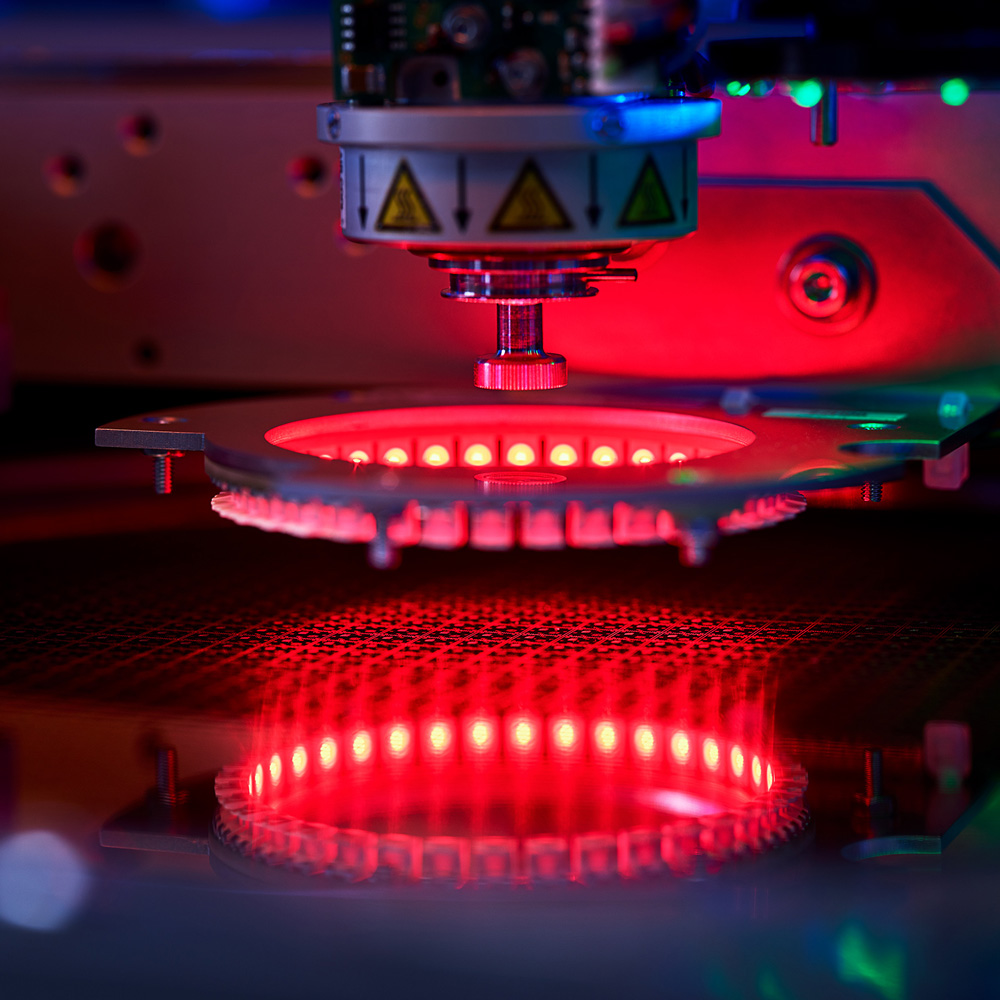
Bonding
- 0.5 – 25N closed loop bond-force
- 0-360° bond rotation
- Heated bond head (max. 450°C) (option)
- UV curing with up to 2,000mW/cm2 (365 / 405nm) (option)
Bonding
- High-end auger pump
- Time pressure dispensing
- Piezo jetter valves
- Pin transfer
- Auto epoxy volume control
Specifications
The Datacon 2200 evo advanced in numbers
Accuracy
| X/Y placement accuracy | ± 3 µm @ 3s |
| Theta placement accuracy | ± 0.07° @ 3s |
| Bond Force | 0.5 N to 25 N programmable |
Output
| Die attach | up to 7,000 UPH/module |
| Flip Chip with dipping | up to 2,500 UPH/module |
| Flip Chip without dipping | up to 3,200 UPH/module |
Bond heads
| Standard bond head | 0° – 360° rotation |
| Heated bond head | up to 450°C (optional) |
| UV curing | 365 nm & 405 nm |
System dimensions
| LxDxH | 1,160 x 1,225 x 1,750 mm |
| Weight | 1,300 kg |
Statistics
| Uptime | > 98% |
| Yield | > 99.95% |
Wafer handling
| Die size – die attach | 0.15 – 30 mm |
| Die size Flip Chip | 0.5 – 30 mm |
| Die thickness | > 50 µm (thinner on request) |
| Wafer size | 4 – 12″ (SEMI M1) |
| Frame size | FF070, FF105, FF108, FF123; automatic change (others on request) |
Chip tray handling
| Waffle pack / Gel pack | 2 x 2″ and 4 x 4″ |
| JEDEC tray | on request |
Substrates and carriers
| Substrates | FR4, ceramic, BGA, flex, boat, lead frame, waffle pack |
| Carriers | Gel-Pak®, JEDEC tray, odd-shape substrates |
| Substrate working range | 13” x 8” (325 mm x 200 mm) |
Options
| Hardware | Open platform architecture for full customization |
| Software | Single component tracking, CAD download, wafer mapping, substrate mapping, barcode scanner, datamatrix recognition and more |
