
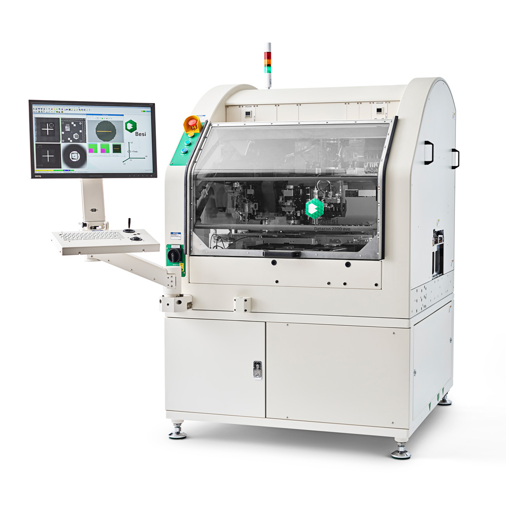
Datacon 2200 evo hS
The Datacon 2200 evo hS is a high-speed, fully automatic die bonder designed for advanced semiconductor packaging applications.
Featuring precise placement accuracy and versatile bonding capabilities, it supports a wide range of die sizes and materials.
Engineered for maximum throughput and reliability, the Datacon 2200 eco hS is ideal for high-volume production environments requiring consistent quality and efficiency.
More informationThis link leads to an external website.


7 micron Accuracy, @ 3 sigma
± 0,1° Theta placement
450°C Heated bond head
99.95% Yield
Key Features
Eplore all features of the Datacon 2200 evo hS
Multi-chip
- Fully automatic cycle for Multi-chip production
- Up to 7 Pick & Place tools (optionally 14), 5 eject tools
- Pressure/time (Musashi®), Auger, Jetter type dispensers available
- Epoxy stamping option
- Filled and unfilled epoxy, wide viscosity range
Accuracy
- New high-speed image processing unit
- Full alignment & Bad mark search
- Pre-defined fiducial geometry & customized teaching
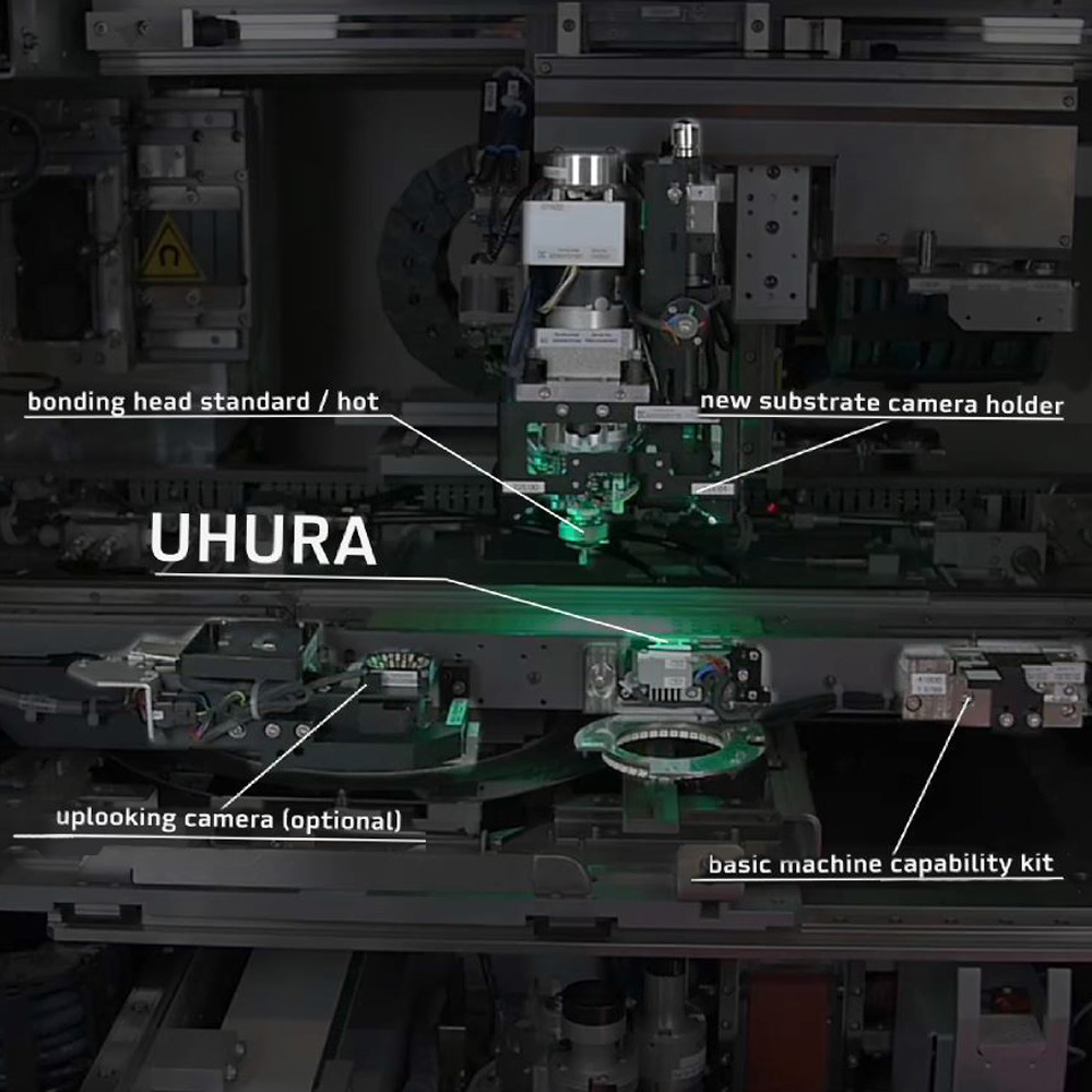
Pick & Place head
- Die Attach and Multi-Chip in one machine
- Die pick from: wafer, waffle pack, Gel-Pak®, feeder
- Die place to: substrate, boat, carrier, PCB, leadframe, wafer
- Hot and cold processes supported: epoxy, soldering, thermo-compression, eutectic
Specifications
The Datacon 2200 evo hS in numbers
Accuracy
| X/Y placement accuracy | ± 7 µm @ 3s |
| Theta placement accuracy | ± 0.10° @ 3s |
| Bond Force | 0.5N to 75N programmable |
Output
| Die attach | up to 12,000 UPH/module |
Bond heads
| Standard bond head | 0° – 360° rotation |
| Heated bond head | up to 450°C (optional) |
System dimensions
| LxDxH | 1,160 x 1,225 x 1,750 mm |
| Weight | 1,300 kg |
Statistics
| Uptime | > 98% |
| Yield | > 99.95% |
Wafer handling
| Die size – die attach | 0.18 – 5 mm (hS mode) |
| Die thickness | 0.05 – 2 mm |
| Wafer size | 4 – 12″ (SEMI M1) |
| Frame size | FF070, FF105, FF108, FF123; automatic change (others on request) |
Chip tray handling
| Waffle pack / Gel pack | 2 x 2″ and 4 x 4″ |
| JEDEC tray | on request |
Substrates and carriers
| Substrates | FR4, ceramic, BGA, flex, boat, lead frame, waffle pack |
| Carriers | Gel-Pak®, JEDEC tray, odd-shape substrates |
| Substrate working range | 13” x 8” (325 mm x 200 mm) |
Options
| Hardware | Open platform architecture for full customization |
| Software | Single component tracking, CAD download, wafer mapping, substrate mapping, barcode scanner, datamatrix recognition and more |
